
Driven by the continuous expansion of AI computing power and cloud services, global data center construction is scaling up rapidly. High-speed optical modules, as the core components for optoelectronic signal conversion, form an essential part of computing network infrastructure. The industry is witnessing a rapid iteration of product speeds—evolving from 100G, 200G, 400G, and 800G toward 1.6T, while 3.2T specifications have already entered the pre-research stage. The overall performance of an optical module depends on several critical technologies, including photonic chips, integrated packaging, thermal management, and electromagnetic compatibility. The higher the transmission rate, the greater the manufacturing difficulty. The internal components of 800G and 1.6T optical modules are highly integrated within compact structural spaces. Even a minor assembly deviation can trigger failure modes such as optical loss, signal bit errors, and wavelength drift, imposing strict mass-production requirements on the performance of automated packaging equipment.

Core Components & Packaging Process Requirements
The optoelectronic conversion function of an optical module is primarily realized through four core units: the TOSA (Transmitter Optical Subassembly), ROSA (Receiver Optical Subassembly), signal processing chips, and PCBA circuit boards. This kind of manufacturing scenario requires micron-level precision assembly: an optical alignment offset of 3 μm will cause beam divergence and exacerbate coupling loss; a 5°C fluctuation in ambient temperature will lead to wavelength drift in the laser, directly impacting reliability.
Due to device miniaturization, variables such as component assembly tolerances, adhesive shrinkage during cure, placement pressure, and dispensing consistency all directly affect yield. The equipment must possess micron-level positioning capabilities, stable dispensing output, and closed-loop placement pressure control to ensure long-term stability of optical coupling.
In the optical module assembly process, dispensing and placement technologies are widely applied in critical stations such as device fixation, cavity protection, moisture-proof sealing, and heat dissipation. Key applications include:
· Protective cover bonding: Sealing dispensing for housing, these are protective covers to block dust and moisture from entering the module cavity.
· Wirebond encapsulation: Applying adhesive over wirebonds to reduce the risk of wire breakage caused by vibration and protect from environmental impact.
· Optoelectronic device bonding & fixation: Adhesive positioning of optical components such as TOSA/ROSA and lenses to lock in the optical coupling position.
· Module sealing: Dispensing and sealing of housing seams to achieve dust and moisture protection for the entire unit, meeting environmental reliability specifications.
· EMI shield cover bonding: Precision placement and dispensing of shielding covers to suppress electromagnetic crosstalk between high-speed signals.
· Chip Underfill: Underfill for DSP and photonic chips to relieve solder joint stress and increase vibration resistance and improve thermal cycling performance.
· Thermal adhesive dispense: Applying thermal interface materials between chips and the housing to dissipate the heat generated from increased temperature of processors , addressing thermal management challenges in high-power modules.
Industry Mass Production Pain Points
The domestic optical module industry is characterized by rapid product iteration, high-mix low-volume production, and short delivery cycles. Traditional fully integrated equipment, which integrates dispensing, placement, and curing processes into a single machine, has exposed numerous limitations in actual mass production.
The cost of whole-machine procurement and maintenance is relatively high. A failure in any of the functional units causes the entire system to stop, directly reducing production line utilization. Process logic is constrained by the hardware architecture, making it difficult to flexibly adjust according to different product process requirements. Process parameters vary significantly across optical modules with different bandwidths and packaging forms, and integrated machines offer limited parameter adjustment flexibility.
Product changeover and setup can take over 4 hours, making it difficult to adapt integrated machines to mixed production modes that simultaneously involve new product prototyping, small-batch trial production, and large-scale mass production. Later-stage process expansion and upgrading are challenging, and line scalability is insufficient. The industry urgently needs modular, reconfigurable automated packaging solutions that balance micron-level assembly precision, mass production yield, and flexible manufacturing capabilities.
axxon Flexible Process Solution
Addressing these mass production pain points, Axxon has abandoned the traditional all-in-one machine architecture and introduced a Flexible Process solution, offering two deployment modes: standalone units and flexible integrated line configuration, to suit different customer production scenarios.
The solution breaks down dispensing, precision placement, and curing into independent process units. Each unit focuses on optimizing specific process performance, and standardized signal interfaces are used between units.
· Standalone Mode: A single machine performs a single or focused process. Same-process models enable 15-minute rapid changeover and are compatible with 100G–1.6T multi-bandwidth, multi-package optical modules—ideal for R&D prototyping and high-mix low-volume production.
· Multi-Process Line Configuration: Equipment is arranged according to the product process requirements to form an automated line. The integration and commissioning time for a single machine to connect to the line is controlled within 1 hour, targeting medium-to-large volume manufacturing.
This flexible process solution has been deployed by several leading optical module manufacturers, balancing R&D validation and volume production needs while effectively shortening new product introduction (NPI) cycles.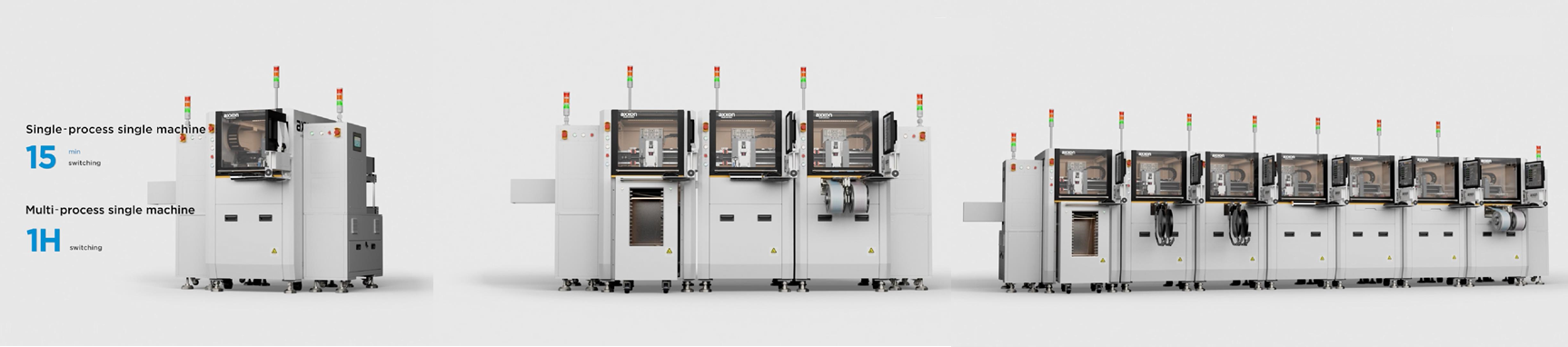
For 1.6T High-Speed Optical Modules
The internal layout of 1.6T optical modules is more compact, with an increased number of dispensing applications, imposing higher standards on dispenser positioning accuracy, placement alignment accuracy, and pressure control.
Leveraging vertically integrated hardware and software-architectures, Axxon achieves closed-loop process control throughout the entire manufacturing process:
1. Dual-head dynamic dual-valve dispensing technology meets micro-distance precision dispensing in extremely narrow areas. Dispenser position accuracy reaches 30 μm, ensuring stable output ofprecisely controlled adhesive volumes and preventing optical component damage caused by overflow.
2. High-resolution vision alignment system, combined with image compensation algorithms, achieves 7 μm placement alignment accuracy, meeting the high-precision assembly requirements of TOSA/ROSA, shield covers, and chip components.
3. 20–100g closed-loop precision force control with accuracy of ±6g prevents placement pressure overload from damaging optical chips and ensures uniform force distribution at the bonding interface.
4. Multi-curing compatibility supports UV curing and thermal curing processes. The curing module can be integrated into the machine or connected as an independent station, adapting to various adhesive process requirements.
Dispensing & Curing
Key Mass Production Metrics
Throughput: 400–500 units/hour
Comprehensive Solution Value
Axxon's Flexible Process, dispensing and placement solution effectively resolves the industry pain point of insufficient flexibility in traditional all-in-one fully integrated production lines. While ensuring micron-level precision assembly capability, it delivers multiple benefits: high precision, high first-pass yield, high equipment utilization, rapid changeover, and easy line expansion.
The solution supports stable mass production of mature 800G products while meeting the development needs of 1.6T and next-generation optical modules. It shortens product introduction cycles, reduces trial production investment, and helps optical module manufacturers navigate rapidly iterating market environments—providing reliable packaging equipment support for computing data center hardware.


